My background in electrical engineering involves the first 4 chapters of an electronics textbook I read on my phone when I had internet connection and power in town while hiking the Appalachian Trail. What can I figure out about how the circuit board works for the quadcopter?
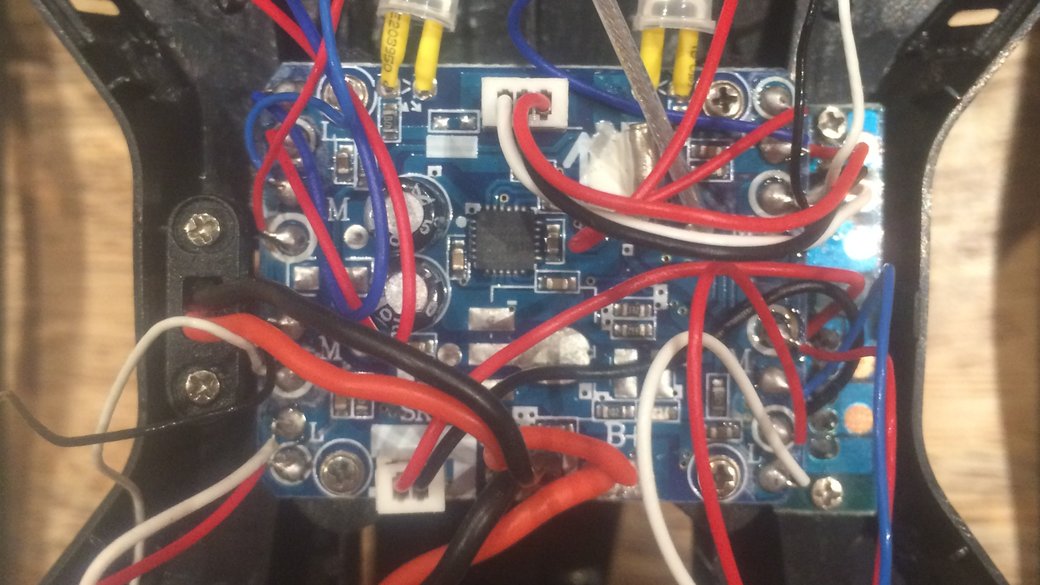
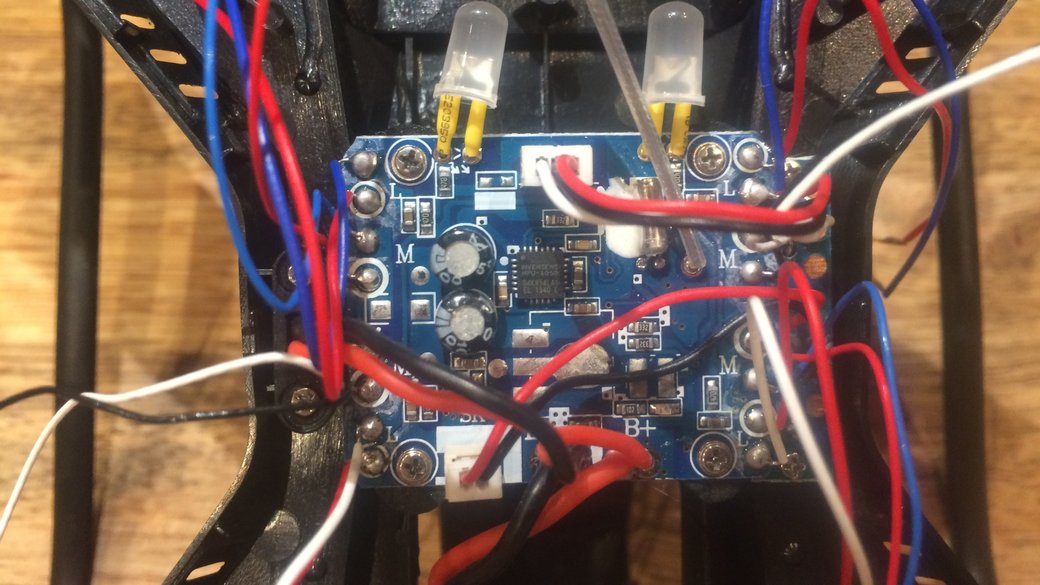
First, some easy wins: The motors are marked with a capital M, and the LEDs are marked with a capital L on the top of the board. I'm guessing this is for soldering on the leads by hand because there's quite a bit of heat melting away at the blue top coat. The other easily identified marks on the top of the board are the B+ and B- for the battery (and charging) leads and an "SK" that appears to lead to the main power switch via a 2 wire connector.
Another interesting note: The camera connector and the power switch are rigidly mounted to the quadcopter chassis, so they're actually on their own separate PCB, probably to reduce the effect that vibration has on the main PCB. The charging port is essentially the same thing, but its just a connector with a handy little physical mount connected by some flexing wire to the main board.
I have some hints from my last article. I also have some general guidance from this handy website I found as the second or third google search result. I can see the major components that are connected off the board, and I can check voltages, but beyond that I'm on my own (and I have to guess at things like checking for a PWM signal).
The IC on Top
Zoom! Enhance!
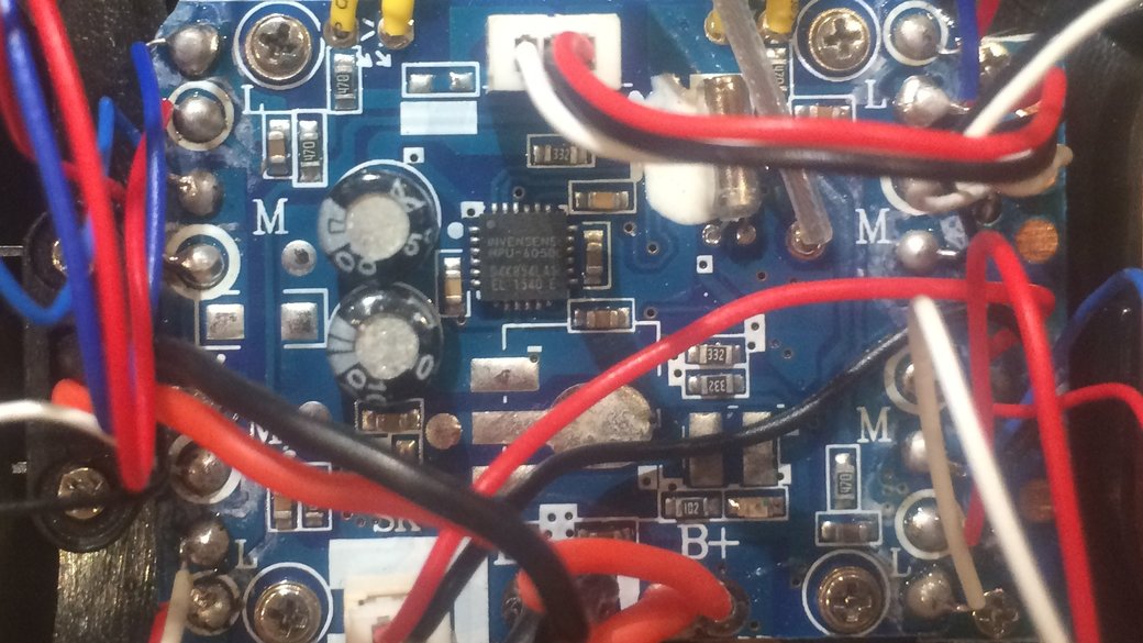
The top of the integrated circuit on top of the board reads:
INVENSENSE
MPU-6050C
D4K854LA1
EL 1540 E
Taking the first two lines, it looks like that part is a 6-axis gyroscope that keeps the whole system stable. Internally, it contains a 3-axis gyroscope and a 3 axis accelerometer built together on the same die, and, according to the website, it's designed to integrate with an external compass (but I haven't found that yet). Additionally, it's designed to work with I2C or SPI for communicating with an application processor; however, it does the onboard sensor processing itself. I'll be interested to see what its "fused" output looks like.
The next line indicate the lot traceability code (D4K...). The next line is a little more complicated, but it indicates FV YYWW R. F is the foundry code, V is the vendor code, YY is the year, WW is the work week and E is the revision. This would indicate that this part was made in late September or early October 2015.
As an additional fun feature for a CS guy, it has a hardware FIFO queue so that the main processor can batch process sensor data if desired and enter a low power mode (or swap threads or something else) while the sensor does its thing.
Reading Specs
From what I can tell, the 050 designation is for the number in the series (60X0) without SPI, so I'm probably looking for an I2C interface.
What do the other numbers on the chip mean?
Can I get any information about the accuracy of the overall fusion algorithm?
The gyro is measured in 131 LSBs/dps. I wasn't sure what the measurement meant, but its essentially a turning rate of 131 of the least significant bits.
Pin out
It looks like there should be a small dot (there is) in the corner with the clock pin and SDA. As I learned reading the datasheet, SDA stands for serial data which comes paired with Serial Clock (SCL). It's not relevant at this point, but I'd be interested in reading a little more into how I2C works.
Continuing counterclockwise in the order of the numbering system for the chip, the next corner holds the pins for connecting to the external sensors (compass?) via I2C. Then you get:
08VLOGIC, the supply voltage for digital communication logic10REGOUT, a pin for a filter capacitor (probably another component on the board)11FSYNC, used for synchronizing with frames for camera stabilization12INT, a digital out interrupt13VDD, power supply voltage18GND, power supply ground20CPOUT, used for connecting to a charge pump capacitor23Serial clock for I2C24Serial data for I2C
The pins I'm most interested in are the REGOUT and CPOUT pins because they should guide me to identifying other parts on the board. Additionally, I'd like to figure out where on the circuit board I can find the ground plane.
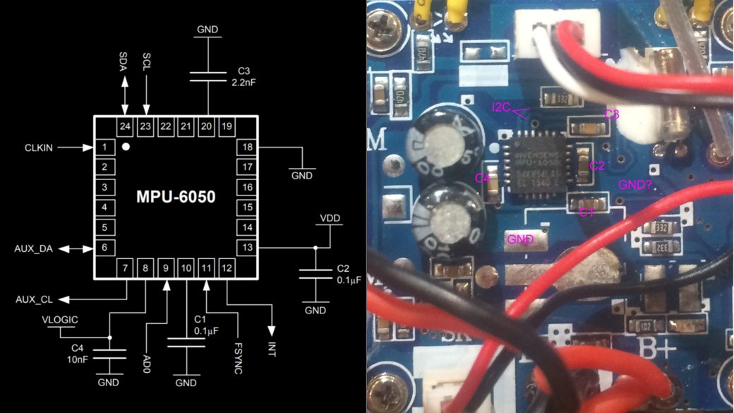
In the image above, one can see the various support capacitors marked, as well as the I2C data pins that lead to the main processor. The last thing that is marked is the ground pins. This is useful for both identifying the rest of the ground plane across the board (no relative voltage, minimal resistance) and the logic and power supplies. The logic supply (VLOGIC in the datasheet) is 1.8V plus or minus 5% (0.09V) and the main power supply (VDD in the datasheet) is 2.375V to 3.46V. Nominally the internal gyroscopes expect 2.5V and probably function down to the 2.375V mark, but this is at the input of an internal charge pump. My guess is that the MEMS need high voltage input but have lower current requirements.
Mildly Interesting
In terms of current, when everything is running on the chip, the chip draws 3.9 milliamps of power. It can drop to as low as 10 micro-amps if just the accelerometer is run at a low update frequency. From reading further, the gyroscope is the power hog, running at 3.6 milliamps.
The gyroscopes are sensitive to high frequency noise in the power supply. Not 100% sure on the units, but it looks like "high" frequency sine waves (250Hz +) in the main power cause a 20x error in gyroscope reading compared with lower frequency input noise. My first guess is that the power supply to the motors (about 3.4V) could also power the gyroscope, but with multiple motors spinning at high rpm, there is the chance for noise in the power input, so maybe not.
Also of note, the offset location of the circuit board does seem designed to place the IMU at the center of rotation for the motors and the center of the frame. This location makes it a lot easier, because it should (in theory) require no extra accounting for a rotational lever arm to convert the accelerations measured by the IMU to the quadcopter frame.
The Bottom of the Board
I've also found a less destructive way to look at the bottom of the board by opening up the battery door, but to really see everything on the bottom of the board, I'm going to need to take out my handy dandy screw driver and lift the board of its vibration reduction mounts.
More next time!
I feel silly, but during this process, I realized that the board has an antenna. Now you know!